Well, my first run through on the simulator with memory and a few instructions worth of microcode and... well, hmmmm.
The instructions seem to work fine until the instruction terminates, and goes back to the fetch instruction, then things fall apart. For some reason, the program counter doesn't seem to be advancing right, or the flip-flops holding each 4-bit word don't seem to be getting the appropriate instruction at the appropriate time.
I'm going to need to do some more experimentation and thought on this one to figure out what went wrong. I have a feeling what I really need to do us use latches instead of flip-flops. More things to play around with. It may make sense to make the registers D-Latches as well, so data is written instantaneously, rather than on a clock tick. Another possibility is using more than one clock, possibly by using some sort of delay line or a secondary clock source.
Wednesday, May 19, 2010

Monday, May 17, 2010
Building a CPU - Musings on the evolution of machine code
Over the weekend I got deeper into some of the more thorny parts of the design. The ALU was really rather simple. For the most part the glue logic was pretty simple. Sure, it looks big and complex, but it's mostly just a bunch of wires that connect from point a to a central routing station to point b, oh, and a few dozen control signals to tell the thing what to do.
This is all fine and good. I can by setting a certain set of inputs instruct the machine to take register o, connect it to bus b on ALU and add it to the accumulator. Great, so the basis of instructions will work.
Now, all I need to do is create an instruction set. At first I had the brilliant idea of using the most significant five bits (8 bit instructions, 2 words) This created a very nice set of 8 bit instructions. I started working out the machine code, how the arguments will be handled and how op-code+arguments will be structured. I knew I was going to somehow index into a set of EEPROMs to get the signals, or a series of signals the op-code will generate. Essentially the EEPROMs would store a table. After fidgeting around with the op-codes and their respective arguments for a while it became painfully apparent that I would either have more ROM for instruction microcode than the entire system has addressable space or I would need some very complex decoding logic to get an index into the appropriate entry into the table.
That simply was not going to work. First, it seems wrong to have several more times address space just to store instructions than the chip is capable of handling from the external world, not only that, but it would be exceptionally sparse, a huge waste of memory. Yes-- memory is cheap these days. ROM is not as cheap, but still rather cheap. The other alternative would mean I'd need a heap of TTL chips to build just the instruction decoder, which aside from requiring large piles of money would also require more power than I care to deal with (I don't really care for needing to add special high-current breakers to the breaker panel, and I don't think the apartment complex would appreciate it.)
So, something had to give. I tried squeezing some different kinds of flags into those eight bits. Hmm, no, that still doesn't work out as cleanly as I would like. I Finally broke down and decided the op-codes between instruction forms will only loosely be related. This means, for example, ld (load a register from memory or another register) would take up about half the available slots, due to the fact that it necessarily needs to move data from anywhere to almost anywhere. st (store register data to memory) is a little bit better in this regard, since the destination is only memory.
Which leaves me with machine code that is functional, but not the orthogonal work of art I had hoped for.
The next challenge was getting some microcode in the simulation to test things out. Unfortunately the banked layout makes things rather nasty as far as just jumping into the sim's hex editor and plopping in codes (notwithstanding the fact that the control word is long enough to tax my memory of what bit handles what, despite the logical ordering of things.) This necessitates some sort of assembler, so I have begun a quick-and-dirty assembler for microcode. This is unlike any other assembly code, the microcode is highly parallel, and needs to perform several operations at once. So each "instruction" becomes a list of instructions followed by either a fetch or next. Fetch will of course read 2 words from the data bus and latch a new instruction. Next will increment an internal counter in the microcode sequencer. As it stands now, each instruction can perform 16 microcode steps. This is, obviously, subject to change as I get a better grip on the requirements of each instruction. 16 seems generous. Some of the instructions in the micro-assembler, will really be a composite of signals, some will be individual signals. Some will simply be modifiers.
I also knew that some of the instruction forms, especially in the forms [si+c], [si+oac], [si+<imm>], [si+<imm16>] would need a bit of new logic in the address bus control, since I didn't think to add the ability to combine addresses with external numbers. This also grows the control word by a few more signals.
I am very glad to be running this through a simulator before beginning the build. It allows me to catch flaws in my design and plan before wiring things up. Before simulations, I'd need to put the whole thing on a breadboard and test it out. Sure, not horrible, but definitely not as quick.
This is all fine and good. I can by setting a certain set of inputs instruct the machine to take register o, connect it to bus b on ALU and add it to the accumulator. Great, so the basis of instructions will work.
Now, all I need to do is create an instruction set. At first I had the brilliant idea of using the most significant five bits (8 bit instructions, 2 words) This created a very nice set of 8 bit instructions. I started working out the machine code, how the arguments will be handled and how op-code+arguments will be structured. I knew I was going to somehow index into a set of EEPROMs to get the signals, or a series of signals the op-code will generate. Essentially the EEPROMs would store a table. After fidgeting around with the op-codes and their respective arguments for a while it became painfully apparent that I would either have more ROM for instruction microcode than the entire system has addressable space or I would need some very complex decoding logic to get an index into the appropriate entry into the table.
That simply was not going to work. First, it seems wrong to have several more times address space just to store instructions than the chip is capable of handling from the external world, not only that, but it would be exceptionally sparse, a huge waste of memory. Yes-- memory is cheap these days. ROM is not as cheap, but still rather cheap. The other alternative would mean I'd need a heap of TTL chips to build just the instruction decoder, which aside from requiring large piles of money would also require more power than I care to deal with (I don't really care for needing to add special high-current breakers to the breaker panel, and I don't think the apartment complex would appreciate it.)
So, something had to give. I tried squeezing some different kinds of flags into those eight bits. Hmm, no, that still doesn't work out as cleanly as I would like. I Finally broke down and decided the op-codes between instruction forms will only loosely be related. This means, for example, ld (load a register from memory or another register) would take up about half the available slots, due to the fact that it necessarily needs to move data from anywhere to almost anywhere. st (store register data to memory) is a little bit better in this regard, since the destination is only memory.
Which leaves me with machine code that is functional, but not the orthogonal work of art I had hoped for.
Control logic: Easy at first but maybe not on closer inspection
So I began work on the instruction decoder after I put together an instruction set. One of the things I knew would be a requirement is that the EEPROMs be banked. Allow me to explain: The control word is ~50 bits wide. Each micro-instruction is a control word. EEPROMs generally have an 8 bit data bus. I could fetch in series each chunk of microcode and bring it into a final register, but this complicates things and wastes precious instruction cycles. So, rather than a single EEPROM, I'll need 7. As far as the decoder is concerned, it's not a big deal. The tricky part is getting an 8 bit instruction from a 4 bit data bus. This has to be done in two cycles. Also, during this cycle the current micro-instruction must stay the same, or the decoder could lose its fetch signal. So, the decoder pulls an op-code in two cycles, and once the cycle is complete it then latches the op-code. Upon latching, the first micro-instruction of that op-code now sends its signals out to the rest of the CPU. That latch step added one clock to the fetch cycle. A necessary evil, I suppose.The next challenge was getting some microcode in the simulation to test things out. Unfortunately the banked layout makes things rather nasty as far as just jumping into the sim's hex editor and plopping in codes (notwithstanding the fact that the control word is long enough to tax my memory of what bit handles what, despite the logical ordering of things.) This necessitates some sort of assembler, so I have begun a quick-and-dirty assembler for microcode. This is unlike any other assembly code, the microcode is highly parallel, and needs to perform several operations at once. So each "instruction" becomes a list of instructions followed by either a fetch or next. Fetch will of course read 2 words from the data bus and latch a new instruction. Next will increment an internal counter in the microcode sequencer. As it stands now, each instruction can perform 16 microcode steps. This is, obviously, subject to change as I get a better grip on the requirements of each instruction. 16 seems generous. Some of the instructions in the micro-assembler, will really be a composite of signals, some will be individual signals. Some will simply be modifiers.
I also knew that some of the instruction forms, especially in the forms [si+c], [si+oac], [si+<imm>], [si+<imm16>] would need a bit of new logic in the address bus control, since I didn't think to add the ability to combine addresses with external numbers. This also grows the control word by a few more signals.
I am very glad to be running this through a simulator before beginning the build. It allows me to catch flaws in my design and plan before wiring things up. Before simulations, I'd need to put the whole thing on a breadboard and test it out. Sure, not horrible, but definitely not as quick.
Thursday, May 13, 2010
Building a CPU - The beginning
So I got the brilliant idea to build a CPU from scratch. So, I'm well into the design phase of this project now, and have a pretty good start. I've designed the ALU, and have some of the control circuitry done.

The diagram above shows the ALU circuitry. Bus A and Bus B serve as the inputs. The shifter can only accept input from bus a, the complementor can accept inputs from either bus. All feed into the result bus, additionally the complementor can feed into the second argument of the adder.
The ALU is capable of performing logic functions (AND, OR, XOR) complementation (NOT, and two's complement) shifting, rotating and addition. Other operations will need to be composites of existing operations. The shifter can shift, rotate, shift with a carry in, and rotate through carry. The flags unit determines which of the 4 flag bits should be active. Results will be placed on the results bus.
Multiplication and division are not available in the ALU, but could be emulated in software using shifts and addition. The ALU also works on signed values, and the shifter can be set to sign extend or not. With signed values subtraction becomes simple addition.
Below is the control circuit. This is not complete as of yet, but may give some insight into how it all works together.

You'll notice it all looks overwhelmingly complex. It isn't really. There are a ton of control lines to direct the ALU what to do, control the registers, and control where the data goes. Unfortunately, the simulation software doesn't allow for sub circuits to have pins that serve as both an input and an output, so there are double the lines on the circuit. You can see that the address bus is 16 bits wide, and the data bus is 4 bits wide.
The CPU has the following registers: Four Bit: A (Accumulator), O (Operand) FLAGS, C (Counter), 16 bit: PC (Program Counter), SI, DI (source and destination addresses). Additionally, there are two registers for the stack. These combine on the data bus to form a 16 bit address, SP and BP. BP is four bits wide, SP is 12 bits wide. This allows for 4k of stack. The placement of the stack is restricted to 4k boundaries, but the BP register allows some flexibility in the placement of the stack, depending on how external memory is configured. The control word will come from a microcode sequencer.
Some of this design is likely to change, and there are some mistakes. the ALU should only be wired to accept input from the accumulator and another register, and will output to a temporary holding latch, which will then store the value in the register. This means the basic operations can complete in two clock cycles. As the diagram is now, it does not function. The data bus controller can only direct data from once source to one destination, and both of the ALU busses are connected to this controller.
Sunday, January 24, 2010
Growing Crystals = Fail
 Lets say for a moment you and your kids decide to do a science experiment. You want to grow crystals. Great! There are lots of resources out there that tell you how to do all sorts of crystals. One of which is salt. Ordinary Table Salt.
So you and your family set out to grow beautiful cubic crystals. You heat up some water, and dump tons of salt in the water until nothing will dissolve anymore. You pour your supersaturated solution of good old sodium chloride into a cup, and dangle a string in the cup. You wait..... and wait... and wait. A week passes, and you have nothing to show for it at all. The sugar crystals came out great, but sugar is so pedestrian. The cubic salt crystals would have been so much better, but it's a total no-go. What happened?
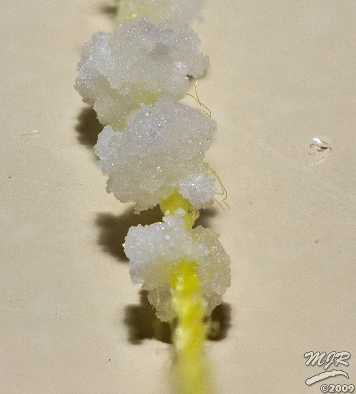


The next stage will be to take an ideal specimen from the crystals formed by the solution and attach it to some nylon fishing line to use as a seed for the final large crystal. Stay tuned!

Tuesday, November 10, 2009
It just keeps getting better: More about the "Lunk Alarm" gym
So, in this detailed review of Planet Fitness, the reviewer goes through all of the amenities, including— get this— Free Pizza and bagels:
Come to think of it, what a great business plan, keep 'em fat so they keep coming back. Augh, I think I'm gonna be sick.
Perks: Free Pizza, Bagels and Candy?
In addition to the free tanning and Shiatsu massage chairs that come with a the Black Card upgrade, Planet Fitness offers three other perks to all of their members: free pizza once a month, free bagels once a month and the ever-present jar of purple Tootsie Rolls at the front desk.
Yes. I’m not joking.
When you join Planet Fitness to get in shape, once a month they reward you for those 300 calories you just burned on the treadmill with a nice 500 calorie slice of greasy, cheap pizza from a local pizzeria. Or how about a giant, high-glycemic carb bagel to set you on your way to great summer abs? And when you’re done working out each day, grab a couple of purple Toostie Rolls loaded with high fructose corn syrup.
This whole thing would be laughable if it wasn’t so absurd. I can understand providing some kind of “treat” to your customers every once in a while, but outside of serving fried chicken or corn dogs, I can’t think of two more unhealthy foods to offer. A better approach would be to provide some type of healthy snack for their members, that helped them get an idea that eating better can taste good as well. Why not wraps, high-fiber protein bars, or even a healthy version of pizza?
Come to think of it, what a great business plan, keep 'em fat so they keep coming back. Augh, I think I'm gonna be sick.
"Judgement Free" Zone
C'mon! get real... A Lunk Alarm?
Ok, Given I'm not in the greatest shape, and I just recently joined a gym (which does not have such an alarm, btw) I've never felt intimidated by the heavy lifters at my gym, but to actually call out and humiliate people with a big blue flashing light and an alarm because they grunt or drop a weight. Give me a break!
Ok, Given I'm not in the greatest shape, and I just recently joined a gym (which does not have such an alarm, btw) I've never felt intimidated by the heavy lifters at my gym, but to actually call out and humiliate people with a big blue flashing light and an alarm because they grunt or drop a weight. Give me a break!
Monday, November 02, 2009
Tainted Candy
Halloween has come and gone. I'm sure many parents out there have closely inspected their kids' loot and given their seal of approval. So how did it happen that we became so careful about our kids' candy? This article gives the incident that set up x-rayed candies, and carefully checking packages for any sign of tampering. Not that you shouldn't be careful about your kids' treats-- you should, but it was someone's own avarice-driven poisoning of their own child that started the whole panic about tainted treats.
Now, that just begs the question: What kind of sick freak poisons their own child to satisfy their own greed!!?
Now, that just begs the question: What kind of sick freak poisons their own child to satisfy their own greed!!?
Friday, October 30, 2009
H is for Hypocrite
If you're going to pass judgment on somebody, first make sure you're not being a hypocrite.
Monday, October 26, 2009
Buyer Beware
This falls under the subject of predatory advertising.
I follow Mouse Print pretty closely, reading their weekly articles. They've covered such things as airline's hidden fees and ways food manufacturers disguise their downsizing. The article linked above is, in my opinion, the worst that it gets. A web page that purports to be an actual news article from a real news organization touting the benefits of some dietary supplement.
Many people could be fooled into thinking it's real, but the entire thing is a work of fiction created by a bottom-feeding supplement manufacturer. I have seen similar websites for similar products. All seem to espouse the benefits of the product and appear on the surface to be legitimate. That is, of course, until you look at the fine print buried at the bottom of the page.
Shame on them.
Oh, and by the way: There is no magic berry that can make you lose weight. Losing weight is simple math, You have to take in less calories than you use.
Wednesday, October 14, 2009
Half-baked
So, imagine this:
A happy couple sits down with a cake decorator, and describes what they want. A wedding cake with a traditional lace pattern, but with a twist, hidden in the lace would be a subtle ninja star. Oh, by the way, it would be fun to hide small ninja figures in the fondant apricots. Sure! No problem! replies the baker. Imagine the shock and dismay when presented with the final result on your wedding day.
A happy couple sits down with a cake decorator, and describes what they want. A wedding cake with a traditional lace pattern, but with a twist, hidden in the lace would be a subtle ninja star. Oh, by the way, it would be fun to hide small ninja figures in the fondant apricots. Sure! No problem! replies the baker. Imagine the shock and dismay when presented with the final result on your wedding day.
Subscribe to:
Posts (Atom)